
It is well known that all metals exposed to air will be oxidised. In order to prevent PCB copper pads from being oxidised, the surface of the pads should be coated (plated) with a protective layer.The material, process and quality of the PCB pad surface treatment directly affects the soldering process and soldering quality. In addition, the choice of PCB pad surface treatment varies depending on the electronic product, process and welding material. Songsheng Optoelectronics will discuss the influence of PCB pad coating on laser soldering.
The influence of PCB pad coating material on laser soldering is mainly reflected in the following aspects:
Anti-oxidation and contamination: In order to prevent PCB copper pads from being oxidised and contaminated before soldering, it is usually necessary to treat the pad surface with a protective coating (plating). This coating can effectively protect the copper surface and extend its solderability.
Chemical composition of coatings: Different coating materials have a significant impact on weld quality. For example, ENIG Ni(P)/Au coatings, a commonly used weldability coating, have a chemical composition that includes nickel and gold, elements that improve the corrosion resistance and weldability of the coating. Coatings with moderate phosphorus content (e.g., 7 to 9 per cent phosphorus) have better corrosion resistance and solderability.
Density and structure of the coating: The density and structure of the coating can also affect the quality of the solder. If the structure of the coating is not dense enough, this may lead to the phenomenon of "black discs", i.e. cracks or voids on the surface of the coating, which may affect the welding result.
Optical properties of the coating: The optical properties of the coating, such as absorbance and reflectance, also affect the results of laser soldering. The electrical resistance coefficient and the surface condition (finish) of the material affect the absorbance of the light beam and thus the soldering process.
Physical properties of the coating: The physical properties of the coating, such as hardness and adhesion, also affect the quality of the weld.
The impact of PCB pad coating materials on laser soldering is multi-faceted, including anti-oxidation, chemical composition, structural density, optical properties and physical properties. Choosing the right coating material and process is the key factor to ensure the quality of laser soldering.

ENIG Ni(P)/Au Coating
1) Coating Characteristics ENIG) Ni(P)/Au (chemical nickel and gold plating) process is carried out after the PCB is coated with a soldermask (green oil). The basic requirements for the ENIG Ni/Au process are solderability and reliability of the solder joints. Chemical plating thickness of 3 to 5 μm, chemical plating Au layer (also known as dip Au layer, replacement Au), the thickness of 0.025 ~ 0.1 μm. chemical plating thick Au layer (also known as reduction of Au layer), the thickness of 0.3 ~ 1 μm, generally in the 0.5 μm or so.
The P content of chemical nickel plating is crucial for the weldability and corrosion resistance of the coating. Usually contains P 7% ~ 9% suitable (medium phosphorus). P content is too low, the coating corrosion resistance is poor, easy to oxidise. And in corrosive environments, because of the corrosive effect of Ni/Au on the primary cell, it will have an effect on the Ni/Au Ni surface layer is corroded, resulting in Ni black film. (NixOy), which is extremely unfavourable to the weldability and the reliability of the solder joints.P content is high, the corrosion resistance of the plating is improved, and the weldability can be improved.
2) Application Characteristics
High cost
●Black disc problem is difficult to eradicate, the rate of defective soldering tends to remain high.
Reliability of secondary interconnections on ENIG Ni/Au surfaces is inferior to that of coatings such as OSP, Im-Ag, Im-Sn, and HASL-Sn.
● Because ENIG Ni/Au using Ni and 5% to 12% P plated together, so when the PCBA operating frequency exceeds 5GHz, the effect of skinning is very obvious, because Ni-P in the signal transmission of the composite coating of the conductivity is worse than copper, and therefore the signal transmission speed is slower;;
● The ENIG Ni/Au surface is dissolved into the brazing surface, the secondary interconnect reliability and OSP is higher, Im-Ag, Im-Sn and HASL-Sn coatings are less reliable.
Gold brittleness" is a hidden danger that reduces the reliability of solder joints. Generally speaking, the soldering time is very short and can only be completed in a few seconds, so Au cannot be evenly diffused in the solder, and therefore a highly concentrated layer is formed locally with low strength.
2.Im-Sn Coating
1) Coating properties Im-Sn is a very important in recent years in the process of non-lead solderability coating. sn chemical reaction (stannous sulphate or stannous chloride) to obtain the thickness of the Sn layer between 0.1 and 1.5 μm (after a number of soldering at least soaked Sn thickness should be 1.5 μm). This thickness is related to the concentration of stannous ions in the plating solution, the temperature and the porosity of the coating. Since Sn has a high contact resistance, it is inferior to immersion silver testing for contact detection testing. With the conventional Im-Sn process, the coating is grey in colour, and due to the honeycomb arrangement of the surface, it results in more porosity, easy penetration and accelerated ageing.
2) Application characteristics
● more expensive than ENIG Ni/Au and Im-Ag, OSP low; ● more expensive than ENIG Ni/Au and Im-Ag, OSP low.
●Tin whisker problem exists, which has a greater impact on fine pitch and long-life devices, but has little impact on PCB; ●Tin plague phenomenon exists.
●Tin plague phenomenon exists, Sn phase transition point is 13.2 ℃, below this temperature turns into powdery grey tin (α tin), so that the loss of strength.
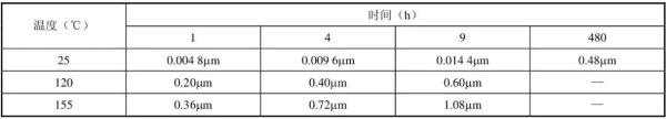
●In temperature environments, SnCu intermetallic compounds accelerate diffusion with the copper layer, causing SnCu intermetallic compounds (IMC) to grow as shown in Table 1; and
● New boards have good wettability, but after storage for a period of time, or after several re-flows, the wettability decreases faster, so the back-end application process is poor.

● As shown in Table 2, after high-temperature treatment, the storage time is reduced due to the depletion of the tin layer thickness
3.OSP coating
1) Coating properties OSP is the emergence of Cu surface organic flux protection film (hereinafter referred to as OSP) in the 1990s. Some cyclic nitrogen compounds, such as benzoquinone triazole (BTA), imidazole, alkyl imidazole, benzoquinone imidazole, and other aqueous solutions are easily reacted with a clean Cu surface. The nitrogen heterocycles in these compounds form complexes with the Cu surface and this protective film prevents oxidation of the Cu surface.
2) Application Characteristics
● Low cost and simple process.
●When soldering is heated, the copper complex decomposes rapidly, leaving only bare copper, because OSP is only a molecular layer that is decomposed by dilute acid or flux when soldering, so there is no residue contamination; ●When soldering is heated, the copper complex decomposes rapidly, leaving only bare copper.
Better compatibility with leaded or lead-free soldering
OSP protective coating is compatible with flux RMA (medium activity), but not with less active rosin-based no-clean flux; ● OSP protective coating is compatible with RMA (medium activity), but not with less active rosin-based no-clean flux.
● OSP thickness (currently mostly 0.2 ~ 0.4μm) on the selected flux matching requirements, different thicknesses of flux matching requirements are also different; ● OSP thickness (currently mostly 0.2 ~ 0.4μm) on the selected flux matching requirements; ● OSP thickness (currently mostly 0.2 ~ 0.4μm) on the selected flux matching requirements
●High storage environment condition requirement, short workshop life, if the production management can not match, it can not be selected.
4.Im-Ag coating
1)Coating propertiesAg has good thermal conductivity, electrical conductivity and weldability at room temperature, strong reflective ability, low high frequency loss and high surface conductivity. However, Ag has a high affinity for S, the atmosphere has a small amount of S (H2) S, all SO2 or other sulfides will change the colour, resulting in Ag2S, Ag2O loss of weldability. another disadvantage of Ag is that in a humid environment, Ag ions can easily migrate along the surface of the insulating material and the direction of the volume, which reduces or even short-circuits the material's insulation properties.
Ag deposited on the base material copper is 0.075 to 0.225 μm thick, with a smooth surface for lead bonding.
2) Application characteristics
● Relatively inexpensive compared to Au or Pd.
●Good lead bonding and good solderability with Sn-based brazing alloys; ●Intermetallic compounds are formed between Ag and Sn (Ag3Sn) without significant susceptibility.
●Intermetallic compounds formed between Ag and Sn (Ag3Sn) have no significant friability.
●In radio frequency (RF) due to the skin effect in the circuit, Ag's high conductivity characteristics just exerted; ●In radio frequency (RF) due to the skin effect in the circuit, Ag's high conductivity properties
●When contacting with S, Cl, and O in the air, AgS, AgCl, and Ag2O are generated on the surface, respectively, which darkens the surface by losing luster and affects the appearance and solderability.
How to optimise the density and structure of PCB pad coating to improve the efficiency of laser soldering?
In order to optimise the density and structure of PCB pad coatings to improve the efficiency of laser soldering, the following aspects can be considered:
Coating Selection:
Choosing the right solderability coating is critical. For example, ENIG Ni(P)/Au coatings provide good solderability and solder joint reliability, and this chemical Ni/Au plating process is performed after the PCB is coated with a soldermask (green oil). This coating provides higher solder quality and efficiency.
Pad design:
The symmetry of the pads is critical to ensure that the surface tension of the molten solder is balanced. The pads must be symmetrical at both ends to ensure that the solder is evenly distributed during the soldering proce
The shape and size of the pads also need to be carefully designed. For example, pads with apertures greater than 1.2mm or pad diameters greater than 3.0mm should be designed as diamond or plum shaped pads. These special shaped pads can better accommodate large size components and reduce thermal stress during the soldering process.
Pad spacing:
Ensure that the component ends or pins and pads of the appropriate lap size, to avoid pad spacing is too large or too small, which will affect the quality of the soldering. Reasonable pad spacing can ensure that the solder can flow evenly during the soldering process, forming a good solder joint.
Optimisation of laser welding process parameters:
Optimisation of laser welding process parameters, such as laser power, welding speed and defocusing amount, is the key to improving welding quality and efficiency. By adjusting these parameters, the laser beam can be made more concentrated and the energy density can be increased, thus speeding up the welding speed and improving the quality of the welded joints.
Minimum size of one side of the pad:
According to the PCB standard package library, the minimum of one side of the pad is not less than 0.25mm, and the maximum diameter of the entire pad is not greater than 3 times the component aperture. This helps to ensure that the solder can fully fill the pad during the soldering process and form a strong solder joint.
Songsheng Optoelectronics laser thermostatic soldering real-time temperature feedback system, CCD coaxial positioning system and semiconductor lasers are composed of; original PID on-line temperature regulation feedback system, can effectively control the thermostatic soldering, there is a real-time high-precision control of the temperature of the object to ensure that the soldering yield and precision. Especially suitable for temperature-sensitive high-precision soldering processing, customers can need free samples!
Contact: Mr.Xiao
Phone: +86-13385280662
E-mail: market001@whlaser.cn
Add: Room 02, Floor 5, Building 9, Gezhouba Sun City, No. 40, Gaoxin 4th Road, Donghu New Technology Development Zone, Wuhan