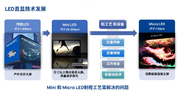
Mini LED and Micro LED (also known as μLED) refer to LEDs with chip sizes smaller than 200 μm and 50 μm, respectively. Like traditional LEDs, they are self-luminous and are typically used in direct display applications of various sizes. Each pixel can be illuminated by an RGB LED chip, which produces three distinct colors. In terms of technology and display advantages, Mini and Micro LEDs inherit the beneficial characteristics of standard LEDs. Their energy consumption is only 10% that of LCDs and 50% that of OLEDs, while their brightness is 30 times greater than that of OLEDs, achieving a resolution of up to 1500 PPI. Additionally, they offer high reliability, rapid response times, long lifespan, and fast operational speeds.

It is anticipated that in the next decade, the continued reduction in the size and cost of LED chips, along with significant advancements in processing techniques, will lead to a revolution in backlighting and display technology. Mini and Micro LED technologies are poised to become the ultimate solutions for commercial displays, wearable devices, mobile phones, computers, and more. The evolution of these technologies will inevitably drive ongoing iterations and upgrades in both process and technology. As we transition from Mini LED to Micro LED, the size of individual LED chips will double, resulting in continuous improvements in display quality and accuracy. Additionally, the number of LED chips utilized in a given area will increase exponentially. For instance, 4K resolution direct display products feature nearly 8.3 million display pixels, which correspond to approximately 24 million LED chips. The sheer volume of chips involved in the panel manufacturing process necessitates significant advancements in transfer, welding, chip repair, and drive control technologies. A new, disruptive process will be required to address these technical challenges effectively. Reason: Improved clarity, vocabulary, and technical accuracy while maintaining the original meaning.
The key steps in the production of MicroLED display panels are as follows:
1.Red, green, and blue LEDs are produced on a transparent substrate growth wafer.
2.LLO: The LED on the growth wafer adheres to the temporary carrier board using adhesive, while the excimer laser focuses through the transparent substrate to separate the LED from it.
3.LIFT: The excimer laser is focused through the temporary carrier plate to selectively separate individual LEDs and transfer them to the designated pad positions on the final substrate.
4.LAB: A semiconductor laser simultaneously heats multiple LEDs and solders to rapidly melt and create a final bond.
5.LFX: Issues with single laser stripping of problematic LED components, application of spot solder paste, and single laser solidification.
The extensive welding and repair system at Songsheng Optoelectronics focuses on three essential aspects of the Mini LED and Micro LED large welding and laser chip repair process, offering an optimal solution for Mini and Micro LED applications.
Spot Control: Songsheng Photoelectric's innovative optical shaping technology enables semiconductor lasers to produce square, linear, or rectangular large spots, as well as precise small spots. Customers can select from standard spot sizes or customize spot parameters based on their specific needs. This customization allows for effective one-time welding across the entire covered area, achieving the goal of large-scale welding, or facilitating precise laser chip repairs with accurately sized spots.
Uniformity: The light field homogenization technology developed by Songsheng Photoelectric achieves a maximum spot uniformity of 99%, with no zero-order diffraction. In actual products, the spot uniformity performance exceeds 97%, effectively ensuring high yield and exceptional consistency in the welding area.
Temperature control :Temperature control in closed-loop systems can effectively simulate the control process of a high-temperature reflux furnace. This approach allows for the editing of temperature curves and facilitates the processes of preheating, warming, holding, and cooling of solder paste.

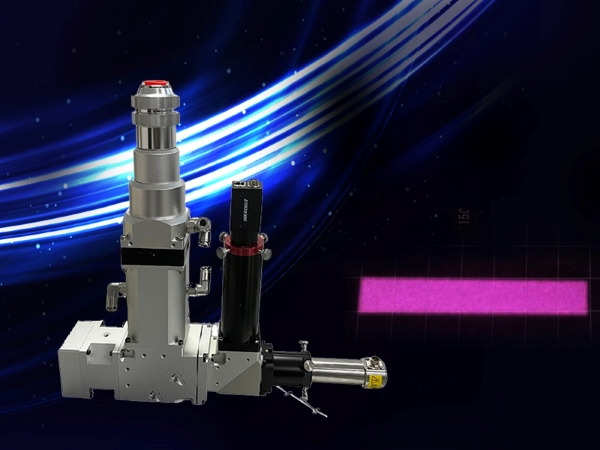
Mini-LED Laser Welding System + Spot Image
Songsheng Optoelectronics MiniLED laser welding system utilizes a 2000W, 976nm wavelength semiconductor fiber laser light source. Through proprietary optical designs developed by Songsheng Optoelectronics, the system employs micro-optical modules to control spot size and achieve optical homogenization. This results in a spot energy uniformity exceeding 97%.

Mini-LED Laser Constant Temperature Repair System with Spot Image
Songsheng MINILED laser constant temperature repair system utilizes a 30-150W power output with a 976nm wavelength semiconductor fiber laser light source. The optical system offers optional focus spot sizes of 253x125, 365x187, 616x305, and 902x440 (±20 microns). The system provides a spot range and energy uniformity greater than 95%.
Contact: Mr.Xiao
Phone: +86-13385280662
E-mail: market001@whlaser.cn
Add: Room 02, Floor 5, Building 9, Gezhouba Sun City, No. 40, Gaoxin 4th Road, Donghu New Technology Development Zone, Wuhan