With the continuous advancement of 5G infrastructure, industrial sectors such as precision microelectronics, aerospace, and shipbuilding have experienced further development, all of which involve the application of ceramic substrates. Among these, ceramic substrate PCBs have gained increasing adoption due to their superior performance. Ceramic substrate serves as the foundational material for high-power electronic circuit structural technology and interconnection technology. They feature a dense structure but also process a certain degree of brittleness. Traditional processing methods, which involve stress during machining, are prone causing fractures in extremely thin ceramic sheets.

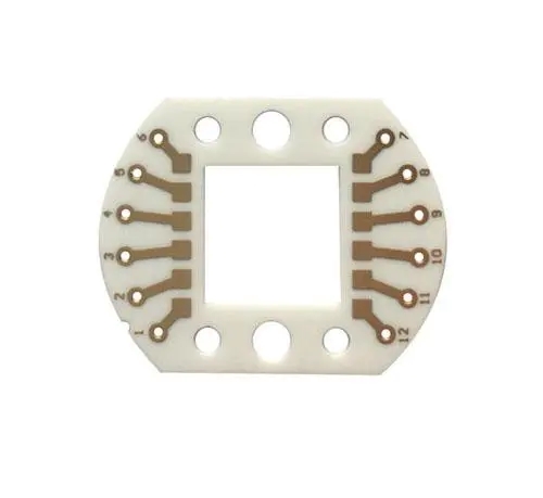
Illustration of Finished Ceramic Substrate Products
Due to the small size and high density of electronic devices and semiconductor components, laser drilling processes are required to meet high standards in terms of both precision and speed. Depending on the specific application requirements of the components, the diameter of microvias typically ranges from 0.05 to 0.2 mm. Currently, laser drilling is widely used for processing ceramic substrates. Pulsed lasers or quasi-continuous lasers (such as fiber lasers) are generally employed for ceramic drilling, with laser spot diameters usually ≤0.05 mm. Depending on the thickness of the ceramic substrate, through-holes of different diameters can be achieved by controlling the defocusing amount. For through-holes with diameters smaller than 0.15 mm, drilling can be accomplished by adjusting the defocusing parameters.

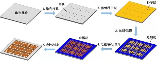
Diagram of Ceramic Substrate Process Flow
Process: Ceramic Substrate
1. Laser Drilling →
2. Seed Layer Sputtering →
3. Photolithography/Development →
4. Electroplating (Filling/Thickening) →
5. Stripping/Etching
Ceramic circuit board cutting primarily involves two methods: waterjet cutting and laser cutting. Currently, fiber lasers are predominantly chosen for laser cutting in the market. Fiber laser cutting of ceramic circuit boards offers the following advantages:
(1) High precision, fast speed, narrow kerf, small heat-affected zone, and smooth, burr-free cutting surfaces.
(2) The laser cutting head does not contact the material surface, preventing scratches on the workpiece.
(3) Narrow kerf, minimal heat-affected zone, negligible local deformation of the workpiece, and no mechanical distortion.
(4) Excellent processing flexibility, enabling the cutting of arbitrary shapes as well as tubes and other profiled materials.

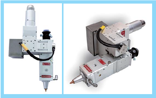
Songsheng Optoelectronics has developed the QCW1064 high-speed rotating precision cutting and micro-hole processing head to meet the demands of precision cutting and drilling. This cutting head is designed for precision fiber lasers (λ=1064nm) and features a multi-lens combination for collimation and focusing, resulting in a small focused spot and high accuracy. When integrated with XY galvanometer scanning and rotation, along with a fiber laser, it enables the cutting of micro-apertures. With an optimized mechanical design, precise adjustment mechanisms, and fully sealed performance, combined with water cooling and coaxial gas assist, the laser cutting head can operate consistently and stably at higher power levels. This product is also compatible with coaxial imaging.
It is capable of drilling micro holes with diameters ranging from Φ0.1 to 0.5mm in ceramic substrates, aluminum plates, copper plates, and stainless steel plates with a thickness below 1mm. With coaxial gas assist, the holes exhibit excellent circularity and smooth edges.
Amid the trends toward miniaturization and thinning, traditional cutting methods can no longer meet the demands due to insufficient precision. As a non-contact processing tool, laser technology offers significant advantages over conventional methods in cutting applications and plays a crucial role in the processing of ceramic substrate PCBs.
Contact: Mr.Xiao
Phone: +86-13385280662
E-mail: market001@whlaser.cn
Add: Room 02, Floor 5, Building 9, Gezhouba Sun City, No. 40, Gaoxin 4th Road, Donghu New Technology Development Zone, Wuhan