Analysis of the Advantages of Laser Soldering for PCB Through-Hole Pads
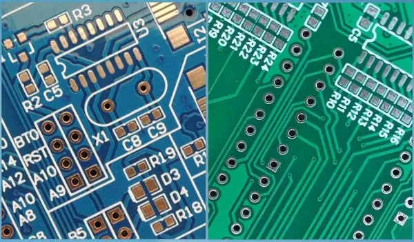
With the growing consumer demand for portable electronic devices, products are becoming increasingly slim and lightweight for enhanced portability and usability. This trend has led to ever-increasing requirements for higher density and miniaturization of PCB circuits. The key to achieving greater PCB density lies in progressively narrower trace widths/spacings, smaller interlayer via diameters/pads, and stricter dimensional tolerances. It is precisely these demands that have driven the introduction of laser welding technology into PCB manufacturing processes.

Songsheng Optoelectronics, as a system integrator with over 15 years of experience in laser soldering, is often asked about the difference between vias and through-holes during PCB prototyping consultations.
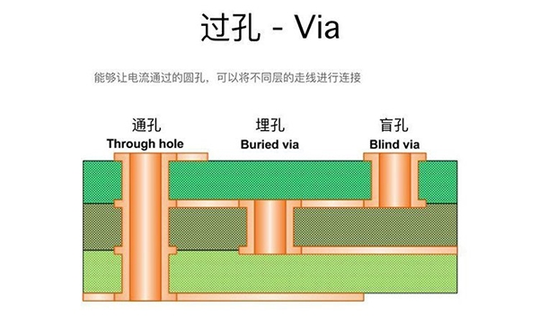
In fact, all holes on a PCB can be called vias. Functionally, vias connect traces between different layers, while through-hole pads secure component leads. Structurally, they can be divided into blind vias, buried vases and through-holes, as shown in the diagram below.

Below we analyze the differences from multiple perspectives:
Blind Via
Located on the top or bottom surface of a PCB with limited depth, connecting surface traces to inner layer traces without penetrating the entire board. The depth typically does not exceed a specified ratio (relative to the aperture diameter). This via type exclusively links inner layer traces to surface layer traces.
Buried Via
An internal connection hole within the PCB that doesn't extend to either surface. Both blind and buried vias are fabricated before lamination using through-hole formation processes, potentially involving multiple overlapping inner layers. Buried vias solely connect traces between internal layers, making them invisible from the PCB surface.
Through-Hole
Penetrates the entire circuit board for either internal interconnections or component mounting. As the most manufacturable and cost-effective option, through-holes dominate PCB designs compared to the other two via types.

Songsheng Optoelectronics Laser Soldering System Overview
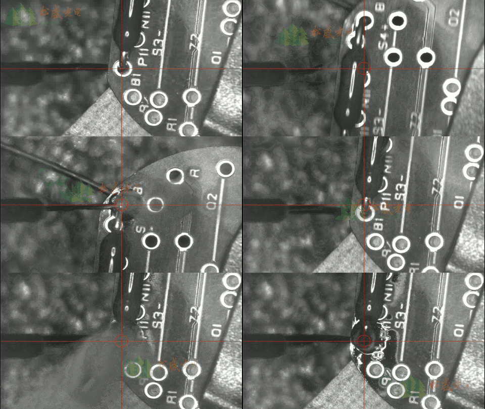
The Songsheng Optoelectronics laser soldering system integrates multi-axis servo modules, real-time temperature feedback, CCD coaxial alignment, and semiconductor laser technology. Through years of process refinement, we have independently developed intelligent soldering software compatible with multiple file formats. Our proprietary PID temperature control system ensures precision constant-temperature soldering, guaranteeing high yield and accuracy for PCB through-hole soldering. The system offers both inline production and standalone operation capabilities with the following features:
Non-contact soldering eliminates mechanical stress and minimizes thermal impact.
Multi-axis intelligent work platform (optional) accommodates complex, precision soldering processes.
Coaxial CCD imaging and monitoring provides clear soldering point visualization and automatic alignment correction for high precision.
Proprietary temperature feedback enables direct control of solder joint temperature with real-time thermal profile display to ensure quality.
Four-point coaxial alignment (laser, CCD, temperature measurement, and guide light) solves multi-optical path alignment challenges without complex calibration.
High-precision soldering achieves 0.2mm minimum solder joint diameter with 99% yield and rapid processing per joint.
Multi-axis flexibility (X/Y/Z) supports diverse component soldering for broader applications.
Contact: Mr.Xiao
Phone: +86-13385280662
E-mail: market001@whlaser.cn
Add: Room 02, Floor 5, Building 9, Gezhouba Sun City, No. 40, Gaoxin 4th Road, Donghu New Technology Development Zone, Wuhan