Considerations on Laser Soldering Process for Gold-Plated PCBs
Why do PCBs require gold plating? As integrated circuit density continues to increase, IC pins are becoming more densely packed. However, vertical hot air leveling (HAL) technology struggles to flatten fine pads adequately, making SMT mounting difficult. Additionally, HAL-finished boards have a relatively short lifespan. Gold-plated PCBs effectively address these issues:

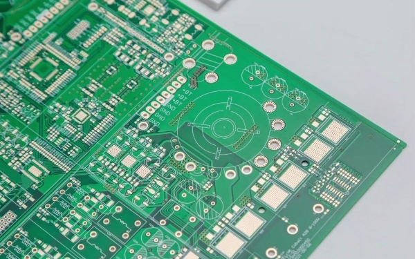
Gold Plating Illustration for PCBs
Enhanced Conductivity: Precious metals like gold possess excellent conductive properties. By applying gold plating, a metallic conductive layer forms at PCB connection points, significantly improving circuit conductivity. This effectively reduces connection resistance, minimizes signal loss, and enhances transmission stability and reliability.
Oxidation/Corrosion revention: The gold plating layer demonstrates exceptional chemical stability, providing superior resistance against oxidation and corrosion. This protective metallic coating safeguards PCBs from environmental contaminants, substantially extending product lifespan.
Improved Solderability: Metal surfaces naturally develop oxide layers that compromise soldering quality. Gold plating significantly reduces oxide layer thickness, ensuring more reliable and robust solder joints. The metallized surface also promotes better solder wettability, reduces thermal stress during soldering, and minimizes soldering defects.
Aesthetic Enhancement: Gold plating elevates the visual appeal of PCBs, enhancing perceived product quality and potentially increasing market value.
While gold is theoretically an excellent solderable coating, in practice, gold-plated parts sometimes exhibit inferior solderability compared to tin-plated or hot-air-leveled (HAL) surfaces. The reasons are as follows:
Porosity Issues in Thin Gold Layers:
When the gold plating is too thin, its inherent porosity allows electrochemical corrosion to occur between the gold layer and its underlying nickel or copper substrate due to their potential difference. This forms an invisible oxide layer on the gold surface.
Organic Contamination Susceptibility:
The gold plating layer readily absorbs organic substances (including organic additives from the plating solution), leading to the formation of an organic contamination layer on its surface.

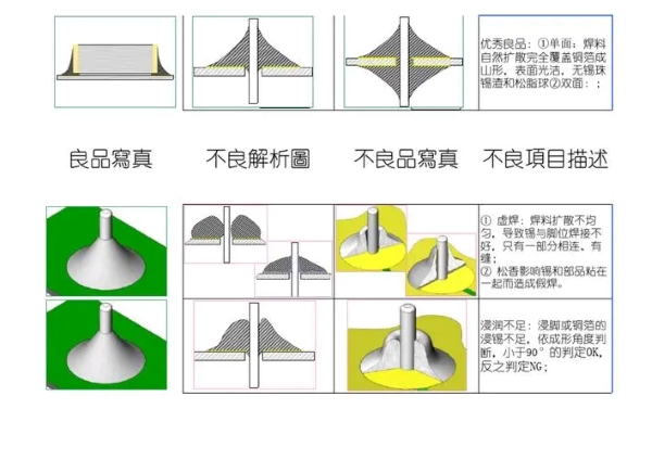
Illustration of Qualified vs. Defective Soldering
Both of these substances can significantly reduce the solderability of gold-plated layers, leading to cold solder joints (commonly referred to as "virtual soldering", which typically indicates a soldering quality defect caused by the inability of the solder to adequately wet the base metal or gold-plated metal due to metal oxides or organic contaminants on the soldered surface).
In today's electronics manufacturing, product quality is increasingly dependent on soldering quality. Among soldering quality defects, cold solder joints rank first in negatively impacting the operational reliability of electronic products.
The phenomenon of cold solder joints is complex in cause, wide-ranging in effect, highly concealed, and results in substantial losses. In practical work, locating a single virtual solder joint often requires significant manpower and material resources. Comprehensive solutions involve multiple aspects and are difficult to establish as stable, long-term remedies. Therefore, virtual soldering has remained a key focus in the electronics industry.
With the widespread adoption of intelligent manufacturing and automated production, many manufacturers have implemented various automatic soldering systems. Among these, laser soldering technology has found extensive application in PCBA. Compared to traditional pressure soldering and soldering iron techniques, laser soldering methods (including laser wire feeding, laser solder paste, and laser solder ball) demonstrate virtually no defective phenomena during operation, such as low solder joint precision, cold solder joints, spikes, missed soldering, or solder ball residue. The primary cause of cold solder joints in laser welding is insufficient dwell time or excessively low temperature of the laser spot on the pad, which can be resolved by extending the laser spot's dwell time or increasing the temperature.

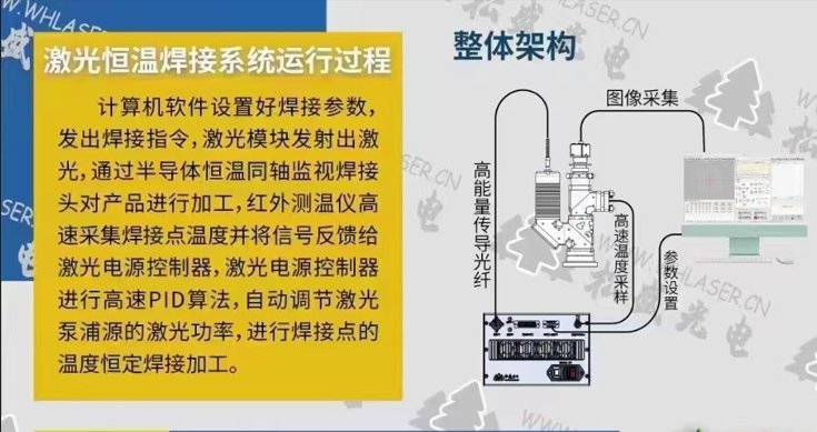
Laser Constant Temperature Soldering System Illustration
Advantages of Songsheng Optoelectronics Laser Soldering System:
Precision Localized Heating
The laser selectively heats only targeted connection points, minimizing thermal impact on substrates and adjacent components. Customizable heating profiles for different component lead types ensure consistent soldering quality.
Rapid Thermal Processing
Features instantaneous heating/cooling cycles that produce dense, reliable joint structures with metallurgically sound connections.
Advanced Non-Contact Technology
Eliminates mechanical stress and electrostatic risks associated with physical contact soldering methods.
Adaptive Heating Control
Programmable heating parameters automatically adjust to component lead configurations, maintaining uniform joint integrity across all nnections.
Micron-Level Manufacturing Precision
Achieves micrometer-scale laser spot control (down to 50μm)
Fully programmable time/power parameters
10x higher precision than conventional soldering irons
Performs reliable soldering in sub-1mm spaces
Superior to both traditional soldering and HOT BAR techniques
Intelligent Optical Alignment
Integrated multi-path coaxial optical system with real-time CCD positioning enables "what-you-see-is-what-you- get" operation, eliminating repetitive vision calibration.
Contact: Mr.Xiao
Phone: +86-13385280662
E-mail: market001@whlaser.cn
Add: Room 02, Floor 5, Building 9, Gezhouba Sun City, No. 40, Gaoxin 4th Road, Donghu New Technology Development Zone, Wuhan