SMD Thermistor Laser Welding Process
日期:2025-05-23
0805 SMD Thermistor Soldering Process
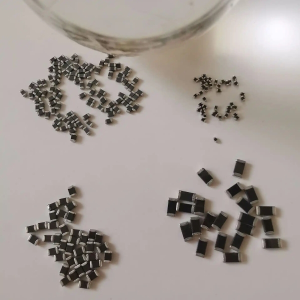
SMD resistors are mainly divided into the following categories: conventional thick film SMD resistors, thin film SMD resistors, high-precision and high-stability SMD resistors, low-resistance SMD resistors, and SMD resistor arrays. Of course, different classification standards result in different categories, such as high-voltage SMD resistors and thick film SMD resistor networks. The figure below shows an NTC thermistor.

0805 SMD NTC Thermistor
This surface-mount NTC thermistor can be simultaneously mounted on circuit boards alongside semiconductors and other passive electronic components. It is particularly suitable for temperature detection circuits in various applications including:
HDD current control
Temperature compensation circuits for optical heads in CD/DVD drives
Temperature monitoring for LED lighting systems
Battery pack thermal management
Key Features of 0805 SMD NTC Thermistor:
• Low capacitance - Ideal for TCXO (Temperature Compensated Crystal Oscillator) applications
• High B-value capability - Compatible with TC20 series specifications
• Glass-sealed surface - Provides enhanced reliability and environmental protection
• Comprehensive product series - Covers diverse application requirements
• Robust glass encapsulation - Ensures superior long-term stability
Pre-Welding Preparation
Component and Material Inspection
It is necessary to confirm that the model and specifications of the SMD thermistor match the design requirements, and to inspect its appearance for any defects such as damage or deformation. At the same time, check whether the welding materials such as solder wire and flux meet the quality requirements, ensuring that the composition and diameter of the solder wire are suitable for the laser welding process.
PCB Pretreatment
Clean the welding area on the circuit board using specialized cleaning agents to remove impurities such as oil stains, dust, and oxides, ensuring good wettability and bonding between the solder and the PCB surface during welding. If there is a solder mask layer on the PCB surface, make sure the solder mask in the welding area is intact, without damage or contamination.
Welding Equipment Adjustment
Adjust the laser welding equipment according to the parameters of the SMD thermistor and the welding requirements. Set appropriate parameters such as laser power, pulse frequency, welding time, and spot diameter. Generally, for laser welding of SMD thermistors, the laser power is typically in the range of tens of watts, the pulse frequency ranges from tens to hundreds of Hertz, the welding time is between a few milliseconds to tens of milliseconds, and the spot diameter is between 0.2 to 1 mm. Specific parameters need to be optimized and adjusted according to actual conditions.
Fixture Preparation
Design and manufacture dedicated fixtures to secure the PCB and SMD thermistor. The fixtures should ensure accurate positioning of the thermistor during the welding process without deformation or displacement caused by the heat from laser welding. The fixture material should have good thermal conductivity and stability to assist in heat dissipation and maintain precision.
Welding Process
Positioning the SMD Thermistor
Accurately place the SMD thermistor at the designated welding position on the PCB and secure it with fixtures. Ensure that the pins of the thermistor are aligned with the pads on the PCB, with a uniform gap typically controlled between 0.05 to 0.2 mm to guarantee welding quality.

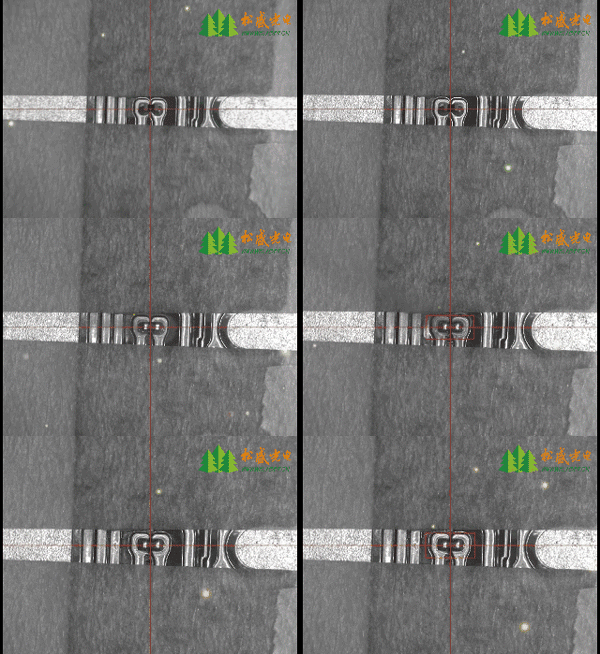
SMD Resistor Laser Solder Paste Welding AnimationFlux Application
Apply an appropriate amount of flux to the contact area between the thermistor leads and PCB pads. The flux serves to remove surface oxides, reduce solder surface tension, and enhance solder fluidity and wettability, thereby improving welding quality. However, excessive flux should be avoided to prevent post-welding residue accumulation on the PCB surface, which may adversely affect electrical performance and appearance.
Laser Welding Operation
Activate the laser welding system and focus the laser beam on the junction between the SMD thermistor leads and PCB pads. Perform welding according to preset parameters, ensuring uniform energy distribution across the welding zone to achieve rapid solder melting and complete wetting of both leads and pads, forming reliable solder joints. For multi-lead thermistors, weld each lead sequentially to prevent component displacement or damage caused by thermal stress during the process.
Welding Quality Inspection
Conduct immediate post-welding visual inspection. Verify that solder joints exhibit bright, plump, and smooth appearance without defects such as pores, cracks, cold joints, or excessive solder accumulation. Confirm secure connections between thermistor leads and pads, checking for any looseness or misalignment.
Post-Welding Treatment
PCB Cleaning
Thoroughly clean the welded PCB using specialized cleaning agents to remove residual flux, solder spatter, and other contaminants. Select appropriate cleaning solutions and methods to prevent damage to both the PCB and thermistor. After cleaning, thoroughly dry the board using compressed air or baking to ensure complete surface dryness and cleanliness.
Electrical Performance Testing
Professional electrical testing equipment such as multimeters and resistance testers shall be employed to conduct electrical performance testing on the soldered SMD thermistor. Measure whether the resistance value of the thermistor falls within the specified range, and verify whether its resistance-temperature characteristics under varying temperatures comply with product specifications. Any abnormalities detected shall prompt immediate root cause analysis and corresponding corrective actions, including rework or component replacement as necessary.
Visual Inspection and Packaging
Perform a final visual inspection of the circuit board to ensure the PCB surface remains clean and all solder joints are defect-free. The assembled boards shall be packaged with appropriate protective measures, including the use of anti-static bags or protective cases, to prevent potential damage from electrostatic discharge or mechanical impact during transportation and storage.
Contact: Mr.Xiao
Phone: +86-13385280662
E-mail: market001@whlaser.cn
Add: Room 02, Floor 5, Building 9, Gezhouba Sun City, No. 40, Gaoxin 4th Road, Donghu New Technology Development Zone, Wuhan