Considerations on Design for Manufacturability in Laser Soldering Processes for PCBA
PCBA (Printed Circuit Board Assembly) represents a critical concept in electronics, denoting the assembled printed circuit board - an indispensable element in modern electronic device manufacturing. The PCBA manufacturing process requires careful consideration of multiple factors to ensure manufacturability, including design specifications, production workflows, quality inspection protocols, and environmental requirements.
Electronics manufacturers universally recognize that preliminary design models fundamentally determine end-product quality. The integration of laser soldering technology with PCBA manufacturability through a "unified design" approach provides essential prerequisites and inherent process capabilities for high-quality manufacturing.
The Design for Manufacturability (DFM) of PCBA intrinsically determines first-pass yield rates in soldering. Its impact on soldering quality is congenital and cannot be effectively compensated through post-hoc process optimization.
DFM directly governs production efficiency and manufacturing costs. Improper PCBA process design may necessitate additional prototyping time and tooling requirements. When design flaws prove irreparable, rework becomes mandatory - all of which degrade production efficiency and escalate costs.
I. Design for Manufacturability (DFM) of PCBA
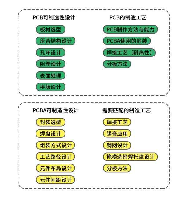
A Printed Circuit Board Assembly (PCBA) refers to a printed circuit assembly component with installed electronic elements that possesses specific circuit functions. As shown in the illustration, it is commonly referred to as a "single board" in electronic manufacturing facilities.

PCB/PCBA Design for Manufacturability (DFM) Illustration
Primary design specifications form the foundation for ensuring PCBA manufacturability. This encompasses PCB design rules including trace width, clearance, aperture size, and pad dimensions - all critical for meeting production requirements.
PCBA DFM primarily addresses ease of assembly challenges, targeting:
Optimized process flow (shortest path)
Maximum first-pass yield
Minimized production costs
Manufacturability of PCBA
The Design for Manufacturability (DFM) of PCB focuses on "manufacturability", encompassing material selection, lamination structure, annular ring design, solder mask design, surface treatment, and panelization design. These design elements are all related to PCB fabrication capabilities. Due to limitations in manufacturing methods and capabilities, PCB processing must meet design requirements for minimum trace width/spacing, minimum aperture size, minimum pad annular ring width, and minimum solder mask clearance. The designed layer stack up and lamination structure must comply with PCB fabrication processes. Therefore, PCB DFM emphasizes alignment with PCB manufacturers' technical capabilities, requiring thorough understanding of PCB production methods, processes, and techniques.
Ease of assembly of PCBA
PCBA Design for Assembly (DFA) focuses on " ease of assembly " - establishing stable and robust processability to achieve high-quality, high-efficiency, and low-cost soldering. Design considerations include component package selection, pad design, assembly methodology (or process route design), component layout, and stencil design. All these design requirements concentrate on achieving higher soldering yield rates, greater manufacturing efficiency, and lower production costs.

II. Laser Soldering Process
Laser soldering technology employs a precisely focused laser beam to irradiate solder pads. The absorbed energy rapidly heats and melts the solder, which then solidifies upon cooling to form reliable joints. This process features localized heating that minimally affects surrounding components, with typical irradiation lasting just hundreds of milliseconds.
The non-contact method eliminates mechanical stress on pads while enabling compact spatial arrangements. The technology achieves precise, controlled heating suitable for high-density PCB applications.

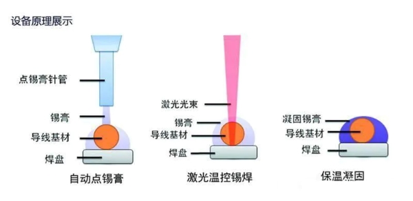
Laser Soldering Process Illustration
Laser soldering technology is specifically designed for selective reflow soldering applications and connector soldering using solder wire. In the case of surface-mount device (SMD) components, solder paste must be precisely applied prior to the welding operation.
The soldering process consists of two distinct phases: initial heating of the solder paste coupled with preheating of the solder joints, followed by complete melting of the solder paste to ensure thorough wetting of the contact pads and subsequent formation of reliable solder connections.
The system incorporates a laser generator with precision optical focusing components, delivering exceptionally high energy density and optimal heat transfer efficiency. This non-contact soldering method accommodates both solder paste and wire formats, demonstrating particular advantages for micro-scale soldering applications within confined spaces due to its low power requirements and energy-efficient operation.

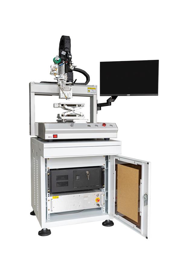
Songsheng Opto Constant-Temperature Laser Soldering System Illustration
The Songsheng Opto constant-temperature laser soldering system delivers continuous 976nm infrared laser output. This integrated system combines a CCD coaxial alignment system with a semiconductor laser module, supporting multiple file formats import to achieve precision soldering. Its integrated temperature feedback mechanism and CCD coaxial alignment capability ensure consistent temperature control during soldering and accurate positioning of delicate components, thereby maintaining high production yield rates.
The system is specifically designed for PCB spot soldering, metal/non-metal material joining, sintering, and heating applications. Its standout feature is real-time high-precision temperature control of the soldering target, making it particularly suitable for highly sensitive precision soldering processes requiring exceptional thermal management.
III. Design Requirements for Laser Soldering in PCBA
Pad Design:
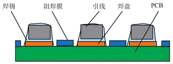
Laser soldering requires pads to be longer than the surface-mounted components to ensure exposed pad areas after component placement, preventing displacement during soldering. The pad and lead structure design directly determines solder joint morphology and molten solder wettability, necessitating proper design to guarantee soldering quality.
Component Layout & Interconnection:
PCBA designs should optimize component placement to minimize interconnection distances, reducing signal attenuation and noise interference. This is particularly critical for laser soldering as shorter connections decrease the heat-affected zone, mitigating soldering deformation and thermal stress risks.
Solder Mask & Stencil Alignment:
Achieving high first-pass yield relies on precise coordination between pad, solder mask, and stencil designs. Proper alignment ensures uniform molten solder distribution and optimal wetting during soldering, enhancing joint quality and reliability.
Thermal Management:
While laser soldering features low heat input, thermal management remains essential for high-power components. Implementation of heat dissipation surfaces, heatsinks, or cooling fans maintains operational temperatures within acceptable ranges, preventing soldering defects or component degradation.
Signal Integrity:
PCBA layouts must prevent signal crosstalk and interference through impedance matching, trace separation, and ground plane design. Though laser soldering's localized heating minimally impacts signals, these considerations remain integral to the design process.
Testing & Inspection:
Comprehensive functional testing and quality verification are essential to validate PCBA designs for laser soldering. This includes solder joint inspection, signal integrity verification, and overall performance evaluation.
In summary, laser soldering imposes specific PCBA design requirements encompassing pad configuration, component layout, solder mask/stencil coordination, thermal design, signal integrity, and validation protocols - all critical for achieving high-quality, reliable solder joints through this advanced process.
Contact: Mr.Xiao
Phone: +86-13385280662
E-mail: market001@whlaser.cn
Add: Room 02, Floor 5, Building 9, Gezhouba Sun City, No. 40, Gaoxin 4th Road, Donghu New Technology Development Zone, Wuhan