Application of Laser Soldering process in PCB Board Welding
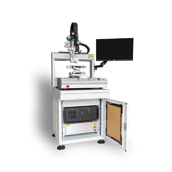
The laser soldering equipment (for solder paste dispensing or wire feeding) primarily consists of several key mechanical components including the solder feeding control system, platform motion system, closed-loop temperature control system, high-speed pyrometer measurement and control system, equipment body and support structure, monitoring and calibration system, laser output control and industrial control system, as well as base and sliding rail mechanisms.
This welding equipment has been widely adopted in factories to achieve automated production. It is mainly used for non-metal welding applications, particularly in the soldering of PCB circuit boards for contemporary consumer electronics products.
The system integrates multiple precision control modules to ensure high-quality soldering results while meeting the demands of modern electronic manufacturing for accuracy, efficiency and reliability. Its non-contact soldering method effectively avoids mechanical stress damage to delicate electronic components.

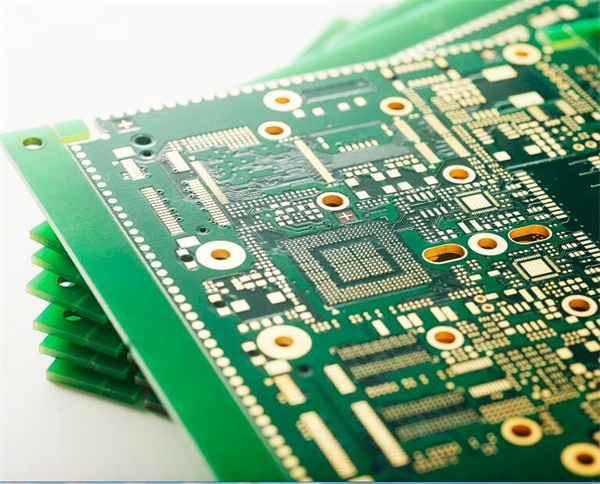
Illustration of PCB Circuit Board
Currently, PCB manufacturers primarily employ four soldering methods: wave soldering, reflow soldering, manual soldering, and automated soldering machines. These methods essentially provide a heating environment to melt solder wire, enabling reliable bonding between surface-mounted components and PCB pads through solder alloy formation. Alternatively, they may utilize electric or electromagnetic pumps to jet molten solder, creating designed solder wave peaks. Another approach involves injecting nitrogen into a solder bath to form waves, allowing pre-assembled printed boards to pass through the solder wave for achieving mechanical and electrical connections between component terminals/pins and board pads via soft soldering.
Post wave soldering and reflow soldering processes typically leave substantial residues on PCB surfaces, causing multiple issues: surface contamination, flammability risks, corrosion, internal layer soldering defects (including missed joints, cold joints, and bridging). Particularly concerning is component vulnerability to deformation, damage, and failure. Repairing PCBs under these high-temperature, large-area conditions proves excessively complex and challenging. While manual soldering and automated soldering machines offer advantages like minimal damage and good precision, they cannot truly support mass production. Manual soldering quality varies by operator, and automated machines present limitations including frequent soldering tip replacements and inaccessible soldering locations.

Songsheng Optoelectronics Laser Constant Temperature Soldering System
To address the shortcomings of conventional soldering technologies, Songsheng Optoelectronics has independently developed a benchtop laser constant temperature soldering system. This advanced equipment features highly automated and precise control systems, delivering continuous 915nm infrared laser output.
The system integrates a CCD coaxial alignment system and semiconductor laser technology, supporting multiple file formats import to achieve precision soldering. With its integrated temperature feedback and CCD coaxial alignment capabilities, the system ensures both constant-temperature soldering and accurate component positioning, thereby maintaining high production yield in mass manufacturing.
Key Features of the Laser Constant Temperature Soldering System:
High-Precision Laser Processing
Minimum spot diameter of 0.1mm enables soldering of micro-pitch mounted devices and chip components
Localized Short-Duration Heating
Minimal thermal impact on substrates and surrounding components
Customizable heating profiles for different component lead types ensure consistent soldering quality
No Consumable Tips
Eliminates heater replacement needs
Enables high-efficiency continuous operation
Micron-Level Precision
Laser spot size reaches micrometer scale
Program-controlled processing time/power parameters
Superior precision compared to conventional soldering irons
Capable of soldering in spaces under 1mm
Six Optical Paths Coaxial Design
Integrated CCD positioning with WYSIWYG (what-you-see-is-what-you-get) functionality
Eliminates repetitive vision calibration
Non-Contact Processing
No mechanical stress associated with contact soldering
Electrostatic discharge (ESD) free
Eco-Friendly Laser Technology
Cleanest processing method with green laser energy
No consumables required
Simplified maintenance and user-friendly operation
Lead-Free Soldering Capability
Eliminates solder joint cracking issues
This advanced system represents a significant technological leap in precision soldering, combining optical engineering, intelligent temperature control, and automated vision alignment to deliver unparalleled soldering performance for modern electronics manufacturing.
Contact: Mr.Xiao
Phone: +86-13385280662
E-mail: market001@whlaser.cn
Add: Room 02, Floor 5, Building 9, Gezhouba Sun City, No. 40, Gaoxin 4th Road, Donghu New Technology Development Zone, Wuhan