Addressing Process Technology Challenges in Mini and Micro LED Manufacturing?
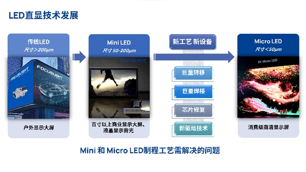
Mini LED and Micro LED (also known as μLED) refer to LED chips with sizes smaller than 200μm and 50μm, respectively. Like conventional LEDs, they are self-emissive and are typically used in direct display applications of varying sizes, where each pixel can be displayed using RGB LED chips of three light-emitting colors.
From technical and display performance perspectives, Mini and Micro LEDs inherit the advantages of traditional LEDs. They consume only 10% of the energy of LCDs and 50% of OLEDs, while achieving a brightness 30 times higher than OLEDs and a resolution of up to 1500 PPI. Additionally, they offer superior reliability, faster response times, longer lifespan, and quicker switching speeds.

The Future of Mini/Micro LED Technology: A Coming Revolution
Over the next decade, as LED chips continue to shrink in size and cost while technical hurdles are progressively overcome, Mini and Micro LEDs are expected to revolutionize backlight and display technologies, potentially becoming the ultimate solution for commercial displays, wearable devices, smartphones, and computers.
The advancement of this technology will inevitably drive continuous iteration and upgrades in manufacturing processes. The evolution from Mini LED to Micro LED has demonstrated that as individual LED chip sizes shrink exponentially, display quality and precision improve significantly while the number of chips required per unit area multiplies.
For example, a 4K direct-view display contains approximately 8.3 million pixels, requiring about 24 million LED chips. This massive scale presents unprecedented challenges in panel manufacturing, demanding groundbreaking innovations in mass transfer technology, high-volume bonding, chip repair sol.
The Key Production Steps for Micro LED Display Panels Are as Follows:
Red, green, and blue LEDs are fabricated on transparent substrate growth wafers respectively.
LLO (Laser Lift-Off): The LEDs on the growth wafer contact and adhere to a temporary carrier with adhesive. An excimer laser focuses through the transparent substrate to separate the LEDs from it.
LIFT (Laser-Induced Forward Transfer): The excimer laser focuses through the temporary carrier to selectively separate individual LEDs and transfer them to bonding pad locations on the final substrate.
LAB (Laser-Assisted Bonding): A semiconductor laser simultaneously heats multiple LEDs and solder to rapidly melt them and form final bonds.
LFX (Laser Fixing): Defective LEDs are individually laser-removed, solder paste is applied, and individual laser die bonding is performed.
Songsheng Optoelectronics' Mass Bonding/Rework System has mastered three critical technical aspects of Mini/Micro LED mass bonding and laser chip repair processes, delivering an optimal solution for Mini/Micro LED manufacturing:
Beam Shaping Technology
Featuring proprietary optical beam shaping technology, Songsheng's system enables semiconductor lasers to output square, linear, or rectangular beam profiles - from large-area patterns to precision micro-spots. Customers can select standard beam sizes or request customized parameters to either achieve single-pass mass bonding across the entire irradiated area or perform precision laser chip repair with micron-level accuracy.
Unparalleled Uniformity
With advanced beam homogenization technology achieving theoretical uniformity up to 99% (with >97% in practical applications) and zero zeroth-order diffraction, the system guarantees exceptional yield rates and consistency across bonding areas.
Closed-Loop Temperature Control
The intelligent temperature regulation system accurately simulates reflow oven processes, allowing programmable temperature profiles that precisely execute the complete soldering sequence: preheating → temperature ramp-up → dwell → cooling.

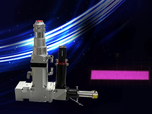
Songsheng Optoelectronics Mini LED Laser Mass Bonding System with Beam Profile Image
Songsheng Optoelectronics' Mini LED laser mass bonding system utilizes a 2000W semiconductor fiber-coupled laser source operating at 976nm wavelength. Through proprietary optical designs with independent intellectual property rights, the system employs micro-optical modules to precisely control both the length and width dimensions of the laser beam spot while achieving optical homogenization with exceptional energy uniformity exceeding 97%.

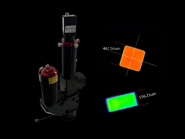
Songsheng Optoelectronics Mini LED Laser Constant-Temperature Rework System with Beam Profile
The Songsheng Optoelectronics Mini LED laser constant-temperature rework system employs a semiconductor fiber-coupled laser source with adjustable power output ranging from 30W to 150W at 976nm wavelength. The system offers selectable spot sizes at the optical focal point: 253*125μm, 365*187μm, 616*305μm, and 902*440μm (±20μm tolerance). Within the irradiated area, the system maintains exceptional energy uniformity exceeding 95%.
Contact: Mr.Xiao
Phone: +86-13385280662
E-mail: market001@whlaser.cn
Add: Room 02, Floor 5, Building 9, Gezhouba Sun City, No. 40, Gaoxin 4th Road, Donghu New Technology Development Zone, Wuhan