How do cold solder joints occur in laser soldering? How to solve them?
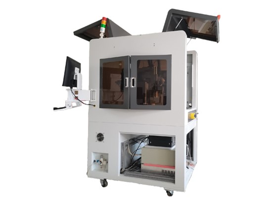
Laser soldering is a highly mature welding technology, but poor parameter control can still lead to soldering defects such as cold solder joints. Songsheng Optoelectronics will explain the causes of cold solder joints in laser soldering and provide solutions.
What is a Cold Solder Joint?
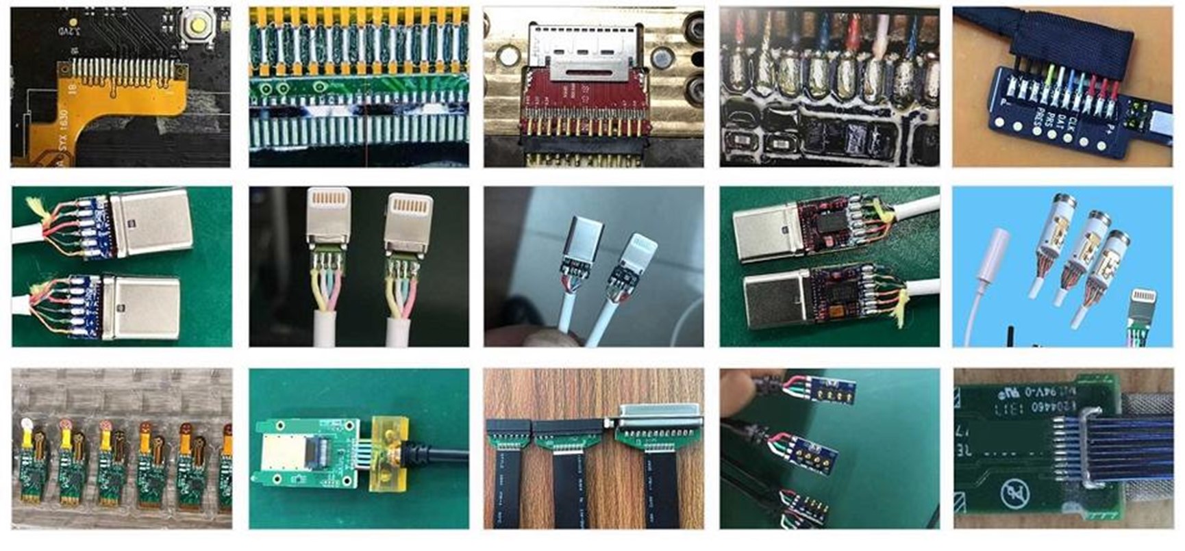
Cold solder joint refers to a soldering condition where the solder and the workpiece surface fail to form a proper intermetallic compound, instead merely clinging to the surface. While appearing properly soldered visually, such joints actually fail to meet requirements in both mechanical strength and electrical performance.
Cold solder joints can significantly reduce the reliability of electronic products. Mechanically, cold solder joints may be unable to withstand normal stress, making them prone to detachment during product use or transportation. Electrically, cold solder joints increase circuit connection resistance, potentially leading to:
Impaired signal transmission
Excessive heat generation
Open circuit conditions
Complete electronic device failure

What Causes Cold Solder Joints?
Material Factors
Poor Surface Treatment of Workpieces
Contaminants like oil stains or oxide layers on workpiece surfaces can prevent proper contact between solder and workpiece. For example:
A thin oil film on electronic component leads makes it difficult for solder to properly fuse with the metal surface during laser soldering, leading to cold joints.
Oxide layers (e.g., copper oxide formed on copper leads in air) are chemically stable. Laser heat may fail to effectively break these layers, preventing proper solder-copper bonding.
Poor Solder Quality
Impure or non-compliant solder composition can cause cold joints. For example:
Excessive impurities in tin-lead solder affect its fluidity and wettability.
Altered melting points or surface tension due to impurities prevent proper solder spreading during laser welding.
Equipment Parameter Factors
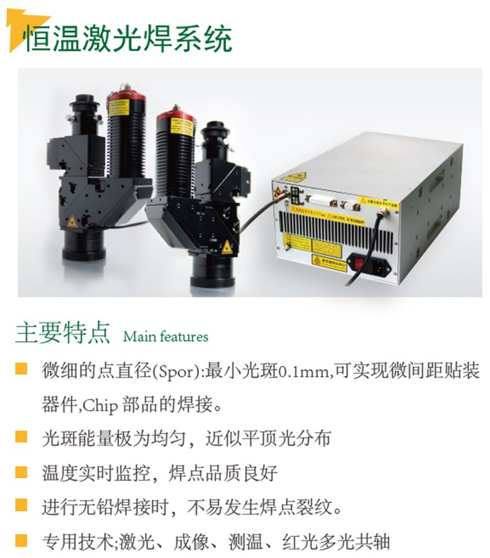
Inappropriate Laser Power
Too Low: Insufficient melting of solder. For precision components, inadequate power results in partial melting, preventing proper intermetallic compound formation.
Too High: Causes excessive solder splatter or workpiece surface oxidation. For PCBs, excessive power can damage copper traces while leaving insufficient solder at joints.

Improper Soldering Duration
Excessively Short Soldering Time
Inadequate duration prevents complete solder melting and wetting of the workpiece.
Example: For thicker workpieces or solder joints, insufficient laser exposure results in incomplete internal melting, causing cold solder joints.
Excessively Long Soldering Time
May lead to solder oxidation, evaporation, or workpiece deformation.
Example: When soldering electronic components with plastic housings, prolonged laser exposure can:
Deform the plastic housing due to heat
Degrade solder quality
Result in cold solder joints

Process Operation Factors
Improper Fit Clearance Between Workpieces
Excessive gap between workpieces makes it difficult for solder to fully fill the joint space.
Example: When soldering a chip to a PCB, if the gap between chip leads and PCB pads is too large, the solder cannot adequately fill the space during laser soldering, resulting in cold joints.
Conversely, insufficient clearance may prevent proper solder flow to the joint area or create air bubbles during soldering, compromising joint quality.
Inaccurate Soldering Positioning
Deviation of the laser beam from the center or critical area of the joint causes uneven solder melting.
Example: When soldering miniature BGA (Ball Grid Array) packages, the laser must precisely align with the chip's solder balls. Even minor misalignment can lead to partial cold joints.
How to Address Cold Solder Joint Issues?
Material Treatment
Clean and Pre-Treat Workpiece Surfaces
Use chemical agents (e.g., alcohol, flux) to remove oil stains.
Employ mechanical polishing or chemical methods to eliminate oxide layers.
Example: Lightly sand copper leads with abrasive paper before soldering, followed by alcohol cleaning, to significantly improve solderability.
Select High-Quality Solder
Ensure the solder’s purity, composition, and performance meet welding requirements.

Equipment Parameter Optimization
Adjust laser power and soldering duration precisely based on factors such as workpiece material and dimensions. Optimal parameters can be determined through experimentation and process refinement. Example: For copper-clad circuit boards of varying thicknesses, conduct small-batch test soldering first, then fine-tune laser power and duration according to the test results until achieving satisfactory soldering quality.
Process Improvements
Maintain Proper Joint Clearance
Strictly control dimensional tolerances between component leads and pads during design and manufacturing.
Example: Ensure precise pad dimensions during PCB production to guarantee appropriate clearance for chip leads.
Implement Precision Positioning
Utilize high-accuracy positioning systems and soldering fixtures to guarantee laser alignment.
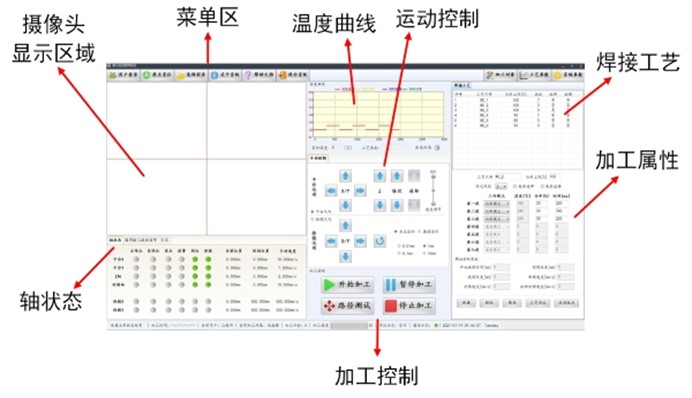
Example: Employ vision alignment systems to calibrate soldering positions pre-welding, ensuring precise laser targeting of solder joints.
Contact: Mr.Xiao
Phone: +86-13385280662
E-mail: market001@whlaser.cn
Add: Room 02, Floor 5, Building 9, Gezhouba Sun City, No. 40, Gaoxin 4th Road, Donghu New Technology Development Zone, Wuhan